all4-PCB translates their significant process experience coming from the printed circuit board industry to the solar industry. Being involved in a highly competitive mass production industry as the circuit board industry provides all4-PCB with significant insight regarding how to find practical and cost efficient solutions for the solar industry. The areas of expertise include all kinds of coating applications and handling large volumes of flat substrates for long dwell time temperature drying or curing process steps.
With locations in Switzerland and Los Angeles CA, as well as significant partners in Asia, all4-PCB has a global reach that allows to facilitate technology transfer between these regions.
Spray Coating Equipment for Wafer Technology
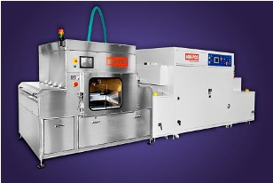
Spray Coating Equipment for Wafer Technology Features:
In today’s world, where wafers are getting thinner and thinner, the solution for the challenges the industry is facing are the contactless coating methods from all4-PCB.Some coating technologies touching your cells for applying process solutions bearing the risk for wafer breakage, decreasing yields and increasing cost.
Other coating technologies are wasting a lot of valuable process chemicals, e.g. spin coating.
Key advantages of the contactless wafer coater for silicon wafers:
- Scalable productivity:
1- 750 wafer/h (from R&D to production in one tool) - Coating thicknesses:
2-20 µm - Storable recipes: 20
- Operation: user-friendly touch panel
- Coating principle: contactless
- Coatingcontrol: control your coating with simply two key parameter
- Software: remote control maintenance with “eyes and ears”
Photovoltaic Contactless Coating Tools for Thin Film Technology
Photovoltaic Contactless Coating Tools for Thin Film Technology Features:
The new all4-PCB tool was designed to produce Activation Layers with or without preheating.
While building thin film solar panels certain technologies require an activation step.
This activation is done mainly with the help of Cadmium Chloride.
Now, all4-PCB introduces its 2nd generation contactless application tool for this process.Their equipment is the safest contactless coating tool available in the world market.
The activation process is boosting the semiconductor efficiency by several percentage points.